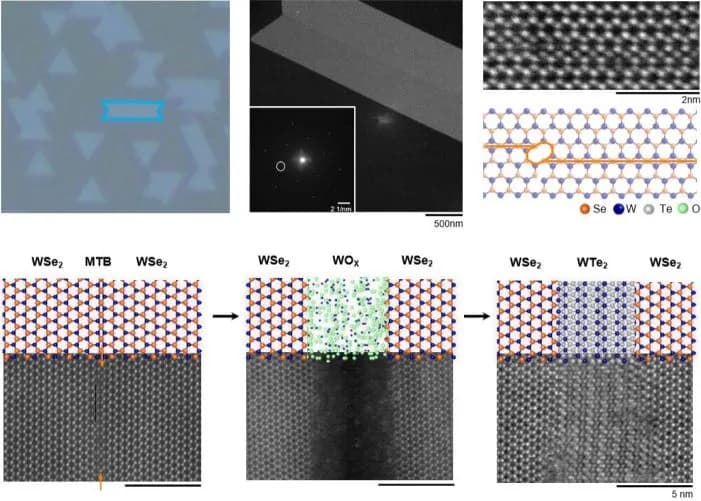
Researchers have built functional MOSFETs entirely within a single tungsten ditelluride (WTe2) monolayer, no external material grafting required. Seok Young Min et al., publishing in Science (doi: 10.1126/science.aei2693), converted discrete regions of the WTe2 top layer into tungsten oxide (WOx) for insulation, n-type WS2, and p-type WSe2, producing a complete transistor structure in-situ at atomic scale.
The significance is density. Silicon transistor fabrication stacks and bonds dissimilar materials across multiple process rounds. This approach sidesteps that entirely, transforming a single crystal layer into all required functional zones. Atomic-scale patterning could push integration densities well beyond what current silicon technology achieves.
WTe2 is not the only candidate. Research into MoSe2 for the same purpose dates to at least 2014 (N. Lu et al., arXiv:1403.3176), and graphene remains an active parallel track. The full paper is paywalled, but the methods section detailing the selective conversion process is where the real engineering lives. That is what you should read.
[READ ORIGINAL →]